Problem/Constraints:
In order to combat controversy concerning the use of paper ballots, as was the case in the Presidential Election of 2000, we were asked to design, prototype, and build, an electronic voting machine capable of accepting and processing four votes from the "companies" board of directors. The companies board of directors consists of a president, vice-president, secretary, and treasurer; each of whom have one vote (yes or no). Majority rule passes a decision, in the case of a tie the President's vote breaks the tie. The voting machine must weigh these inputs, using only AND, OR, and INVERTER Gates, to produce the correct outcome.
Brainstorming
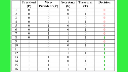
To begin, looking at the problem statement we understand that the President's vote basically counts as two votes, with this knowledge I created a truth table (a table that shows which inputs result in which outputs, in this case which votes result in a passed decision) where a yes vote = 1 while a no vote = 0; and a Passed Decision = 1, while a Declined Decision = 0. From this I was able to write an Un-Simplified Logic Expression (which basically is a list that shows which inputs provide working outputs).
D(1) = P'VST + PV'S'T + PV'ST + PVS'T' + PVS'T + PVST' +PVST
(The commas after certain inputs indicate that it as a zero,
no, or an Xnot).
From this I designed an Un-Simplified Circuit on paper using only AND, OR, and INVERTER GATES
D(1) = P'VST + PV'S'T + PV'ST + PVS'T' + PVS'T + PVST' +PVST
(The commas after certain inputs indicate that it as a zero,
no, or an Xnot).
From this I designed an Un-Simplified Circuit on paper using only AND, OR, and INVERTER GATES
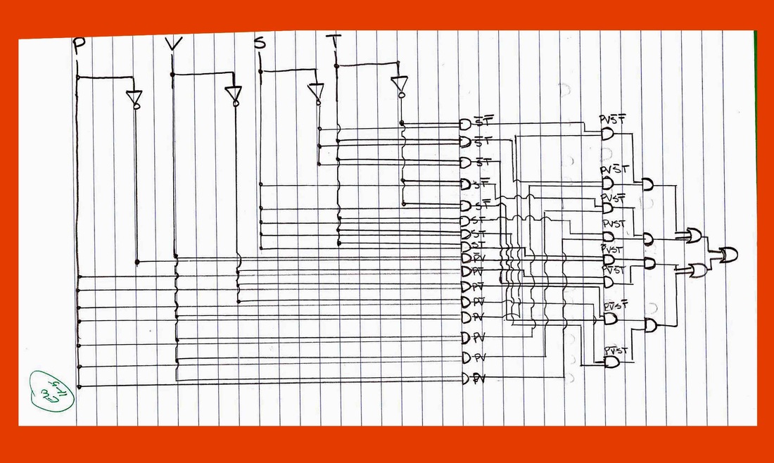
I then built this circuit on MultiSim (circuit building software) in order to test it.
Calculations
After verifying that this circuit worked I was asked to save money by simplifying the circuit, thereby lowering the amount of gates purchased, (not to mention making it WAY easier to wire) I did this by using Boolean Algebra (equations used to simplify circuits) below.
D(1) = P'VST + PV'S'T + PV'ST + PVS'T' + PVS'T + PVST' + PVST
= P'VST + PV'S (T' + T) + PVS' (T' + T) PVS (T' + T)
= P'VST + PV'T(S' + S) + PV (S' + S)
= P'VST +PV'T + PV'S + PV
= P'VST + PV'S + PT + PV
= P'VST + PS + PV + PT
= SVT + PS + PV + PT
D(1) = P'VST + PV'S'T + PV'ST + PVS'T' + PVS'T + PVST' + PVST
= P'VST + PV'S (T' + T) + PVS' (T' + T) PVS (T' + T)
= P'VST + PV'T(S' + S) + PV (S' + S)
= P'VST +PV'T + PV'S + PV
= P'VST + PV'S + PT + PV
= P'VST + PS + PV + PT
= SVT + PS + PV + PT
Final Product
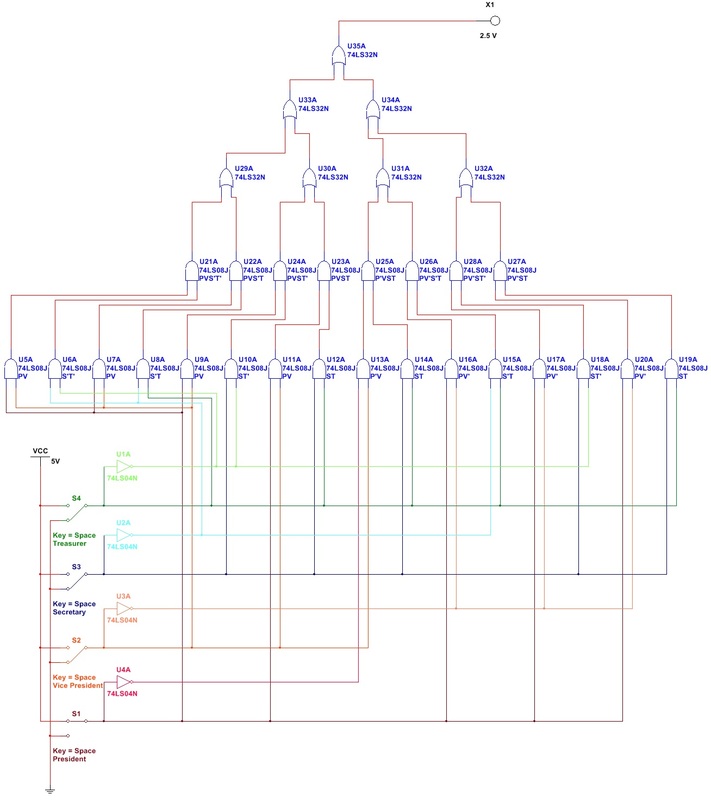
With this new equation I designed a simplified version of the circuit. Which I then tested on multisim and finally built using a breadboard.
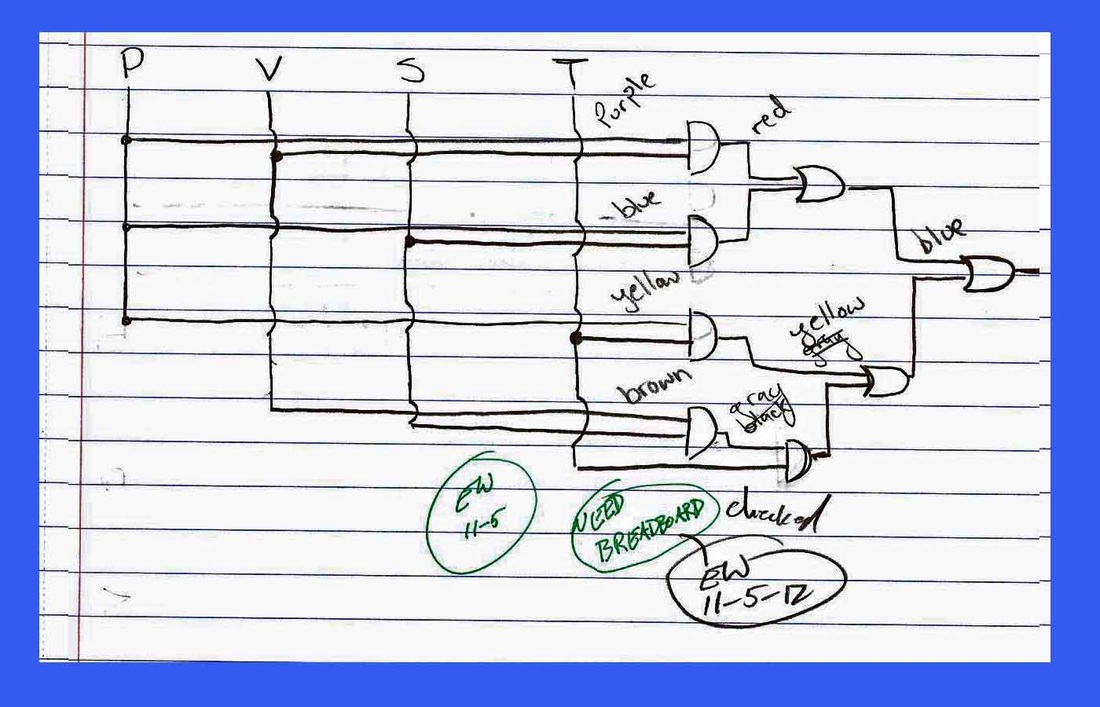
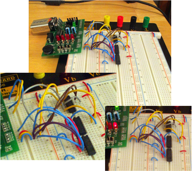
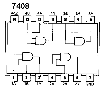
For the breadboard I used physical wires, gates, switches, power, and lights to create a real working version of the voting machine. Basically the important aspects of bread-boarding are color coding your wires (which you can see I noted on the written brainstorm), making sure that they are connected to the right areas, and being able to troubleshoot your circuit if it isn't working. Here is a picture of a "map" of one of the AND gates, showing where an input and output would be connected. Below is a picture of the final working Voting Machine.
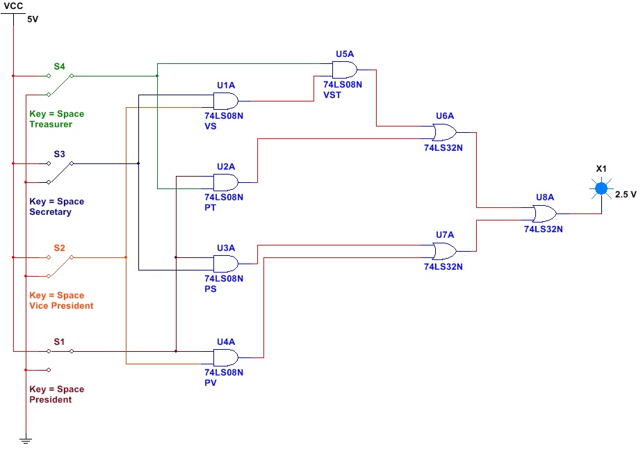
It is operated by flipping 4 different switches: S1 (President), S2 (Vice-President), S3 (Secretary), and S4 (Treasurer). Which are connected to (2) 74LS08 chips / AND gates (which are the top and bottom gates in the picture .... the black boxes in the middle), which are in turn connected to the 74LS32 chip / OR gates (which is the very middle black box), in the formation laid out above. This eventually connects to the first RED LED, which signals that a decision has passed.
Just to clarify the AND gates in the digitally designed circuit are shown as little rectangles with 1 curved end, OR gates are the rectangles with 2 curved ends. The blue light is the LED. Also multiple AND gates fit onto one 74LS08, which will make sense if you look at the "map" I talked about above, the same map applies directly to OR gates, and similarly to INVERTER gates.
Other than that I can't think of any other questions... the small blue and red wires in the picture below supply power and ground to the circuit. Oh and in the equations above, an AND gate is symbolized by multiplication, while and OR gate is symbolized by addition. For more information I am pretty sure I have supplied appropriate hyperlinks everywhere so, go look around if something doesn't make sense. :)
Reflection
Alright so the Edmodo requirements tell me to explain how everything works in this section, but seeing how I have already done that I am going to instead talk about what went wrong. Bread-boarding is really difficult your first few times, as you can see even with color coded wires it still looks a bit messy. That is why you should ideally arrange your wires to go only vertically and horizontally, as well as measure them appropriately. However, for some reason I have anxiety about cutting a wire to short so instead I just color code them and end up with "messy" wire arches going across my board, making things difficult and confusing (for anyone trying to figure out what I am doing). The confusion for ME was caused by the fact that I had my inputs and outputs mixed up on the right side of every chip, which could have been avoided had I referred to the "map" I spoke of earlier. Through this I was able to effectively employ my newly acquired knowledge of bread-boarding, multisim, gate logic, and Boolean algebra.
